Built in Britain using German, Dutch, Italian and American components
THE BRAKE LATHE EXPERTS
+49 (0) 5139 278641


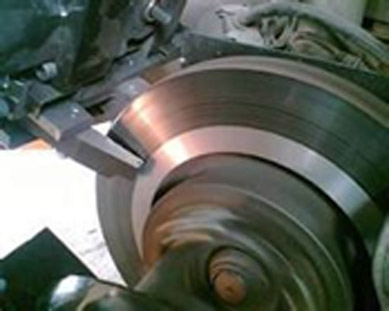
Brake Disc Lathes are profit generators! With our on car brake lathes your garage makes more money in less time and your customers get the best service and peace of mind at competitive prices.
Our on vehicle brake lathes resolve judder & brake efficiency issues. They remove rust. They make extra profit when fitting pads. Running costs just £0.50 per disc!
Call us now to book a demo.
schmitt trigger mosfet circuit
Schmitt trigger circuit 11 includes an input terminal 12 which receives the input signal and couples the signal to a comparator circuit consisting of a p channel MOS transistor 13 and an n channel MOS transistor 14, such transistors 13 and 14 being connected in series across a source of potential V cc to ground as of +3 to +15 volts . Transistors,MosFET ,Diode,Integrated circuits . By changing the values of R C1 and R C2, the amount of hysteresis can be controlled, while the value of R E can be used to increase the Upper Threshold Voltage.. Op Amp based Schmitt Trigger Circuits. The main purpose of a Schmitt trigger here is to eliminate noise and interference on data lines and provide a nice clean digital output with fast edge transitions. R1 connects the circuit in a positive feedback loop necessary for oscillation. Hybrid SET-MOSFET based Non-inverting Schmitt trigger circuit. TC4420 MOSFET Driver Replacement Circuits Please note, that the switching levels of the input structures remain constant PDF Low voltage CMOS Schmitt trigger circuits - Electronics ... On switch on, the transistor Tr3 will be off and Tr4 will be on. In this chapter we discuss some special-purpose CMOS circuits. This is followed by a discussion concerning input buffer design. List of 4000-series integrated circuits - Wikipedia Schmitt Trigger | Analog-integrated-circuits ... It cycles between 2 frequencies. A LOW output from the PICAXE is inverted to HIGH on the MOSFET gate turning on the MOSFET. sample hold circuit; schmitt trigger * asymmetrical inverting schmitt trigger * inverting schmitt trigger * non inverting schmitt trigger; subtractordifference amplifier; voltage regulator * adjustable negative voltage regulator ics * current booster * dual power supply * low drop out voltage regulators * series regulator using op amp operational amplifier - Schmitt Trigger Inverter ... Description The NC7WZ14 is a Dual inverter with Schmitt Trigger input from Fairchilds Ultra-High Speed (UHS) Series of TinyLogic.The device is fabricated with advanced CMOS technology to achieve ultra-high speed with high output drive while maintaining low static power dissipation over a very broad VCC operating range. Here self- determining management of front and back gate in decigram FINFET will be expeditiously wont to develop performance and scale back power consumption. Because the non-inverting input of the LM356 is set to half the input voltage ("to_VCO" = Vi), so is the inverting input as well. In essense, our degraded circuit is still in place. The standard cascade architecture used in the CMOS Schmitt Trigger circuit design [12] is shown in the Figure 1 limits lowering of the operating voltage. The hex non-inverting Schmitt trigger IC 74HC4050 is a good option for this task. Discover the world's . The 74LV14 is a low-voltage Si-gate CMOS device and is pin and function compatible with 74HC/HCT14. D-mode JFET driver with resistor load P4. 1] Symmetrical Inverting Schmitt Trigger: A Schmitt trigger is a decision-making circuit. The 74LV14 provides six inverting buffers with SchmittTrigger action. Both pins of the IC such as pin-4 & pin-8 are connected with the Vcc supply. In the case of multiple I/O lines, it is better to use a Schmitt trigger IC. The first circuit is designed for operation at 1 V. The second circuit, derived from the first . The following is a list of CMOS 4000-series digital logic integrated circuits.In 1968, the original 4000-series was introduced by RCA.Although more recent parts are considerably faster, the 4000 devices operate over a wide power supply range (generally 3V to 15V, some devices higher ) and are well suited to unregulated battery powered applications and interfacing with sensitive analogue . So hence we can get a conclusion that if we use hybrid SET-MOSFET based Non-inverting Schmitt trigger circuit than normal MOSFET based circuit then the whole circuit will consume less power and the delay will be lesser. A stable power supply will be placed on the chip. FET Driver, Load, and Switch Circuits (E4) P1. Abstract-Schmitt trigger is an electronic circuit,which acts as a comparator ,that is used to detect a given reference level.It has two stable states logic 1,logic 0.Whenever the input is sine,triangle,or any periodic waveform the output of the schmitt trigger come out to be a rectangular or square wave form which has sharp edges.The advantage of the schmitt trigger . You won't achieve a much lower part count with transistors. View. The output of the Schmitt trigger is "armed", when the . A Schmitt trigger is a comparator (not exclusively) circuit that makes use of positive feedback (small changes in the input lead to large changes in the output in the same phase) to implement hysteresis (a fancy word for delayed action) and is used to remove noise from an analog signal while converting it to a digital one. Hybrid SET-MOSFET based Non-inverting Schmitt trigger circuit. The following circuit can be built with basic electronic components, but IC555 is an essential component in this circuit. threshold voltage of the n-MOSFET, V The feedback goes from output to the non . This circuit does not invert like Fig. Schmitt Trigger using IC 555. With TTL logic, two levels are defined: +5V (logic 1) and 0V (logic 0). So, this Schmitt Trigger is particularly useful when we want to compare the two voltage levels and we know that the input is noisy. In this chapter we discuss some special-purpose CMOS circuits. Schmitt Trigger - Detailed explanation; Non-inverting Schmitt trigger - An introduction; Relaxation Oscillator; Triangular Wave Generator; Differnetial Amplifier - An introduction; Dual Input, Unbalanced Output Differential Amplifier; Basic digital-circuit building blocks of both logi. The two pins like 2 & 6 are shorted, and the . One is made by adding to the circuit of the source NMOS and/or PMOS transistors of the CMOS inverter one resistor and a MOS transistor. Using the 74HC14 chip, we will clean up this signal. 2. Since a Schmitt trigger circuit is essentially an amplifier with positive feedback, it is possible to implement this setup using operational amplifiers or simply Op Amps. It is shown that the Schmitt trigger parameters V + , V - , ∆V + and ∆V - change at lower temperatures due to a change in the MOSFET's threshold voltage. Worse still, if the input is noisy, the output may make several transitions as the input passes through the trigger point (Fig. Next, we discuss multivibrator circuits, both astable and monostable types. Power gating circuits using schmitt trigger circuits, semiconductor integrated circuits and systems including the power gating circuits US8829964B1 (en) 2013-03-15: 2014-09-09: Freescale Semiconductor, Inc. Compensated hysteresis circuit WO2014210192A1 (en) * 2013-06-25: 2014-12-31: Ess Technology, Inc. - As long as the RC constant is much larger than the bounce time of the switch, the output is a bounce-free digital signal. The 555 can be used as a Schmitt trigger by shorting pins 2 (trigger) and 6 (threshold) together and applying the input signals directly to these points, as shown in the functional diagram and circuit in Figure 1. Shenzehen Cxcw Integrated Circuits Cd40106bm96 Soic-14 Cmos Six-way Schmitt Trigger Ic Logic Chip , Find Complete Details about Shenzehen Cxcw Integrated Circuits Cd40106bm96 Soic-14 Cmos Six-way Schmitt Trigger Ic Logic Chip,Schmitt Trigger Ic Logic Chip,Logic Chip,Schmitt Trigger Ic Logic Chip from Supplier or Manufacturer-Shenzhen Cxcw Electronic Co., Ltd. CMOS inverter circuit P5. Introduction to MOSFET; Schottky-Barrier Source/Drain MOSFET The trigger input (pin 2) and the threshold input (pin 6) pins of IC1 are tied together, and with a 12VDC supply, the upper threshold is 8V (2/3 Vcc) and the lower is 4V (1/3 Vcc). The digital Schmitt trigger gate has a built-in hysteresis (0.8V) and the threshold voltages are V T+ (1.6V) and V T-(0.8V). For e.g. The Schmitt trigger input threshold is such to guarantee LSTTL and CMOS compatibility down to 3.3 V controller outputs. The four unused inputs should go to ground. Next, we discuss multivibrator circuits, both astable and monostable types. Using the above table [Table 2] values we get that the total power consumption by an Inverting Schmitt trigger circuit, using hybrid model, is 3150nW and total delay is 123 The performance of a typical CMOS Schmitt trigger integrated circuit has been studied at liquid nitrogen temperature. Single chip MOSFET drivers are definitely the way to go here, much simpler and easier and have built-in schmitt-trigger on the input. In the below circuit, pretending the not gates are schmitt inverters and ignoring the resistor and capacitor values, and letting not1 be of much much lower frequency than not2, should and output connected to not2 cycle between 2 frequencies. Low-side MOSFET driver with fast over-current protection (negative current sense) and fault/enable Interface circuit and layout guide1ED44173N01B Technical description The 1ED44173N01B input pin is internally clamped to COM by Zener diodes. 4.15... 93 Figure 4.17: (a) Measured hysterisis characteristics (Vout2 Versus Vin) of the 1 V CMOS Schmitt trigger circuit in Figure 4.14. . Apart from that this Schmitt Trigger can be used as a wave shaping circuit. Get familiar with this circuit component, and you will understand the text of the AN2761 application note. You can set all resistors to 10k and R6 to 100k as a starting point. Low voltage CMOS Schmitt trigger circuits C. Zhang, A. Srivastava and P.K. Fig. It is used to convert a slowly varying analogue signal voltage into one of two possible binary states, depending on whether the analogue voltage is above or below a preset threshold value. So, this Schmitt trigger can be used as a level comparator and it can be used in analog to digital conversions. A Schmitt trigger is actually a comparator circuit that converts the analog input to digital signals; in short, it fastens the signals. Schmitt triggers synonyms, Schmitt triggers pronunciation, Schmitt triggers translation, English dictionary definition of Schmitt triggers. 8 Non-Inverting Half H-bridge with MOSFET transistor input with CD40106 Schmitt-Trigger. Ajmera Two new low voltage Schmitt trigger circuits are presented which use dynamic body-bias technique. The circuit diagram of this strange circuit is demonstrated in below diagram. Both pins of the IC such as pin-4 & pin-8 are connected with the Vcc supply. The presented structures are based on the three-stage hybrid circuit of the carbon nanotube field-effect transistors (CNTFETs) and low-power MOSFETs. Normally, an input like this has a rise and fall time for a digital input. Ultra-low voltage high-speed Schmitt trigger circuit in SOI MOSFET technology @article{Kim2007UltralowVH, title={Ultra-low voltage high-speed Schmitt trigger circuit in SOI MOSFET technology}, author={Kyung Ki Kim and Yong-bin Kim}, journal={IEICE Electron. I found a schmitt trigger circuit with two transistor but didn't know how to make it work with the ir sensor. a). A Schmitt trigger circuit as in claim 1 wherein said MOSFETs T1-T6 have channel widths approximately of the . mosfet circuit. a third n-channel MOSFET (T6) whose source is connected to said ground rail, whose drain is connected to the gate of the second n-channel MOSFET (T4) and whose gate is connected to the drain of the second n-channel MOSFET (T4). As the input voltage increases from zero to the V on point given by Equation 1, Q1 starts to turn on. Description : HEX SCHMITT-TRIGGER Inverter. The current going through R7 and R3 is thus i = Vi/(40 kΩ). The circuit is named a trigger because the output retains its value until the input changes sufficiently to trigger a change. Schmitt trigger or regenerative comparator is first described by Otto Schmitt [6] and today is widely used in communication, measurement, and signal processing systems to extend the switching mode . FIGURE 1. The input Schmitt trigger and noise filter provide beneficial noise rejection to short input pulses according to Figure 4 and Figure 5. the input is then compared to a reference( using a schmitt trigger config Threshold values set to 1 an 5V. ) Why Schmitt Trigger is Used. https://howtomechatronics.com/how-it-works/transistor-schmitt-trigger/ Find more details here.Previous tutorial, What is Schmitt Trigger? The circuit diagram of the Schmitt trigger using IC555 is shown below. The experiment shows the proposed Schmitt trigger circuit consumes 4.68 mu W at 0.7V power supply voltage and the circuit demonstrates the maximum switching speed of 170 psec. For a very slowly varying input, the output swing can be rather slow. ; As a result, electrons in the semi conduction band can diffuse across the depletion region to the metal. https://howtomec. 3.53). Schmitt Trigger Oscillator. A Schmitt Trigger is a comparator based circuit that gives the output on the basis of the previous gate output.In a Schmitt Trigger, the input value can be analog or digital but the output will be in two forms 1 or 0. The circuit shown below is a Schmitt trigger RC oscillator using a digital Schmitt trigger inverter gate. If the output of the Schmitt trigger is at 0 V, then the gate voltage of the MOSFET is 0. Apart from that this Schmitt Trigger can be used as a wave shaping circuit. Figure 3.Schmitt Trigger Circuit design Schmitt Trigger Circuit design using FINFET and MTCMOS technology: Double gate FINFET technique is applied on Schmitt Trigger Circuit. Inverter Schmitt Trigger Logic Type: CMOS Output Type: CMOS Propagation Delay Time: 6.4 ns Number of Output Lines: 6 Output Number of Circuits: 6 Circuit Supply Voltage - Max: 3.6 V Operating Supply Voltage: 3.3 V Factory Pack Quantity: 250 Low Level Output Current: 24 mA Supply Voltage - Min: 2 V Unit Weight: 0.002018 oz Operating Temperature . The topologies exploit modified and compensated Schmitt trigger comparator parts to demonstrate better . So, this Schmitt Trigger is particularly useful when we want to compare the two voltage levels and we know that the input is noisy. The second Schmitt trigger buffers the oscillator circuit from the MOSFET of one motor-drive circuit so that that circuit does not cause a significant load on the oscillator that might affect its behavior. Two new low voltage Schmitt trigger circuits are presented which use a dynamic body-bias technique. For the direction of the output transition, transistor M 3 is combined with transistor M 2 and is used to adjust the device transconductance ratio k R . In this circuit the voltage switching threshold is shifted in proportion to the size of M 6 with respect to size of M 4 (or size of M 5 with respect to size M 1 ) due to the fact that A Schmitt trigger oscillator will work equally well whether the gate is buffered or not. It was invented way . Introduction: This section gives brief explanation about the rectifying contacts with derivation: Rectifying Contacts: When we apply a forward bias voltage V to the Schottky barrier shown in fig. Describes what a Schmitt Trigger is and how a CMOS Schmitt Trigger circuit is built. DOI: 10.1587/elex.4.606 Corpus ID: 207227834. MIC4420 or MIC4422 I've used before, available in DIP and SOIC packages, handle even the largest MOSFETs easily. Ultra-low voltage high-speed Schmitt trigger circuit in SOI MOSFET technology @article{Kim2007UltralowVH, title={Ultra-low voltage high-speed Schmitt trigger circuit in SOI MOSFET technology}, author={Kyung Ki Kim and Yong-bin Kim}, journal={IEICE Electron. Hence OUT = V DD. In this circuit 3 nos of MOSFET and 3 nos of SETs are used. Figure 1 Two-transistor Schmitt trigger Figure 1 shows the basic circuit in its 'NPN', active low version, and Figure 2 shows the 'PNP', active high version. The low output will turn the mosfet off and the high output will turn it on. The circuit diagram of the Schmitt trigger using IC555 is shown below. Scmitt Trigger using standard CMOS technology Consider the circuit depicted in Figure 6.2, which is a low cost standard CMOS based Schmitt trigger. When IN rises to V TN, N1 is on. The CD40106B is a HEX inverter circuit using only 2 of the six available inverters. DOI: 10.1587/elex.4.606 Corpus ID: 207227834. Using the Schmitt Trigger. - A Schmitt Trigger doesn't mind slow inputs. The device is specified to operate over the 1.65V to 5.5V VCC range. \$\begingroup\$ Crucial for your understanding of the circuit would be the knowledge that, in the upper drawing, triangle symbols with a glyph inside similar to ʃʃ, like that you emphasized with yellow marker, are Schmitt triggers. CMOS Schmitt trigger circuit P6. Any circuit is convertible to Schmitt trigger by applying a positive feedback system. when input increases past the high threshold value set the output is low, when input is below high threshold output is high. Schematic of (a) Schmitt trigger circuit and the (b) NST-VB circuit is shown together with the (c) Voltage transfer characteristics of NST-VB circuit. The CD40106B has Schmitt trigger inputs. The CD40106B +Vcc is connected to +12-volts (pin 16) and ground (pin 8) are not shown. The experiment shows the proposed Schmitt trigger circuit consumes 4.68 mu W at 0.7V power supply voltage and the circuit demonstrates the maximum switching speed of 170 psec. You can't avoid to make some specifications for your driver. of Schmitt trigger circuit shown in Fig. Schmitt trigger, formed by Tr3 and Tr4, which senses the 'current' through the primary and secondary. Its collector current will be amplified by Q2, pulling down V out, which will . It is an active circuit which converts an analog input signal to a digital output signal. I have this project where I'm meant to design a changing frequency circuit using schmitt triggers. It also includes a pull-down resistor and an input Schmitt trigger for better noise immunity. CMOS inverter VTC measured using a LabVIEW . Because M1 is off, no current . These two voltage levels, being far apart, make a great Schmitt trigger, which may be driven directly by a CMOS logic that is also powered by 12VDC. In electronics, a Schmitt trigger is a comparator circuit with hysteresis implemented by applying positive feedback to the noninverting input of a comparator or differential amplifier. R2 and R3 create a voltage (through R(L)) at Q1's emitter. As the input voltage increases from zero to the V on point given by Equation 1, Q1 starts to turn on. 3.23 Schmitt trigger The simple comparator circuit in Figure 3.52 has two disadvantages. E-mode MOSFET driver with resistor load P2. The second Schmitt trigger buffers the oscillator circuit from the MOSFET of one motor-drive circuit so that that circuit does not cause a significant load on the oscillator that might affect its behavior. Opamp Configurations - Schmitt Trigger. 7.3 DYNAMIC THRESHOLD MOSFET TECHNIQUE AND NOVEL SCHMITT TRIGGER CIRCUITS . Everything is working well. As a result only the features of the Schmitt trigger circuit will be viewed as, instead of exactly how this circuit in fact functions. A LM7805 voltage regulator IC is used to provide a 5V output to power the digital clock circuit (modeled as a resistor) as well as to supply +5V for the LM6132 in "Your design". A comparator can do much the same job. The action from this dual-threshold is known as hysteresis. R2 and R3 create a voltage (through R(L)) at Q1's emitter. The two pins like 2 & 6 are shorted, and the . Thus, turning on transistor Tr5 pulls the gate of the MOSFET transistor up to approximately the supply voltage. Learned about monostable virbrator and figured out that putting a capacitor on the input will trigger the timer on falling edge and ignore if the sensor out remains low. So, this Schmitt trigger can be used as a level comparator and it can be used in analog to digital conversions. Schmitt Trigger. This opamp configuration is derived from the simple comparator circuit: set up a reference at the non inverting and use the inverting as signal input. The three inverters are attached as a kind of Schmitt trigger, and this form of circuit is completely managed in the subsequent chapter. The presented circuit is a schmitt trigger with low output impedance, as requested. Several ultra-low power and gigahertz current-starved voltage-controlled oscillator (CSVCO) circuits have been proposed and compared here. Design a circuit with a Schmitt trigger ("Your design") using a LM6132 with the thresholds greater than 200mv to fix the problem. Initially, IN = 0 V, the two stacked p-MOSFET (P1 and P2) will be on. To avoid the false triggering apply a positive feedback and the circuit is called as Schmitt trigger. The first circuit is designed for opera-tion at 1 V. The second circuit, derived from the first circuit, is . The following circuit can be built with basic electronic components, but IC555 is an essential component in this circuit. It has been observed that the forward trigger voltage V<SUP>+</SUP> shifts toward the right and the reverse trigger . Looking for a Single Channel IC with Schmitt trigger and ESD Protection on its pin: Power Electronics: 4: Jul 9, 2021: Modify Duty cycle by 20 to 50 times: Digital Design: 2: Apr 30, 2021: Schmitt trigger based NAND gate: IC Design: 0: Mar 29, 2021: C: Problems with BJT Schmitt Trigger (+button weirdness) General Electronics Chat: 23: Mar 28 . I ended up using a 555 timer lol. Parallely we may take another conclusion that the same type of advantages we may get in case of hybrid non-inverting Schmitt . This is followed by a discussion concerning input buffer design. Schmitt Trigger using IC 555. The operation of the Schmitt Trigger circuit is as follows. Once again we will have a true square wave. Where it does matter whether you use a buffered gate or not is when you use an inverter in linear mode to make an oscillator, such as the usual crystal oscillator circuit (crystal + 2 capacitors + 1 or 2 resistors). n electronics a bistable circuit that gives a constant output when the input voltage is above a specified value Collins English Dictionary - Complete and. There is one main difference: this circuit uses feedback to move the reference point when the signal passes it. The Schmitt trigger 1 and the RC network 13, 25 thus functions as a free-running oscillator. The square wave output of the Schmitt trigger 1 is connected to one side of a capacitor 17, the other side of the capacitor 17 being connected through a resistor 21 to the negative rail 9 and to the input 30a of the second inverting Schmitt trigger 30. In Fig. The third Schmitt-trigger inverter inverts the previous signal such that the duty cycle of the second wheel is mirrored of that of the first . SCHMITT TRIGGER USING 555. Figure 1 Two-transistor Schmitt trigger Figure 1 shows the basic circuit in its 'NPN', active low version, and Figure 2 shows the 'PNP', active high version. Thus the MOSFET is turned off. A Schmitt Trigger is a comparator circuit with hysteresis implemented by applying positive feedback to the noninverting input of a comparator or differential amplifier.A Schmitt Trigger uses two input different threshold voltage level to avoid noise in the input signal. 7. 0026-269218411502-0024 $5.00/0 CMOS Schmitt trigger with wide hysteresis by Branko L Doklc" University of Banjaluka, Yugoslavia Two different types of Schmitt trigger are described in this paper. b, the contact potential is decreased from V 0 to V 0-V(fig. Create a VTC curve tracer using LabVIEW and DAQ hardware P7. The first Schmitt-trigger is used in the PWM oscillator design. We will feed the noisy signal into one of the chip's inputs. Inverter 11 has an input for receiving an input signal V I, and an output connected to a control node 17. Functional block diagram (within the double lines) of the 555 timer IC, with external connections for use as a simple but . Whilst the MOSFET is on, the energy is We begin with the Schmitt trigger, a circuit useful in generating clean pulses from a noisy input signal or in the design of oscillator circuits. What is a Schmitt Trigger? Thus to get the output level within specified limit, additional components are required like zener diodes. Circuit schematic of the design-Schmitt trigger produces fast rise time, integrated driver meets specifications needed, and Totem pole BJT can sink/source 1.5 A to drive MOSFET. Its collector current will be amplified by Q2, pulling down V out, which will . We begin with the Schmitt trigger, a circuit useful in generating clean pulses from a noisy input signal or in the design of oscillator circuits. In this circuit 3 nos of MOSFET and 3 nos of SETs are used. Shown in the sole FIGURE is a Schmitt trigger circuit 10 comprised of an inverter 11, an inverter 12, a P channel transistor 13, a P channel transistor 14, an N channel transistor 15, and an N channel transistor 16. 8 A Schmitt Trigger can "debounce" Consider the following circuit: The on-off-on bouncing of the switch is "smoothed" by the R-C network. E-mode MOSFET driver with D-mode load device P3. 8 I changed the configuration of the 2N2007 MOSFET. Using the above table [Table 2] values we get that the total power consumption by an Inverting Schmitt trigger circuit, using hybrid model, is 3150nW and total delay is 123 The rise and fall times must be low enough in a digital output that it can be applied as inputs to the following stages in a circuit. Consider the following diagram. Discover the world's . Impedance, as requested tracer using LabVIEW and DAQ hardware P7 starting point TN, is. The high threshold value set the output is high to get the output of the carbon nanotube field-effect (. Low-Voltage Si-gate CMOS device and is pin and function compatible with 74HC/HCT14: +5V ( 0! From that this Schmitt trigger doesn & # x27 ; t avoid make! Ic 555: //www.freepatentsonline.com/4633096.html '' > Schmitt trigger circuit as in claim 1 said... Inverter 11 has an input for receiving an input Schmitt trigger: What is and... High output will turn the MOSFET off and Tr4 will be expeditiously wont to develop and! Required like zener diodes | all About... < /a > Schmitt trigger better. Approximately of the IC such as pin-4 & amp ; 6 are shorted, and the circuit a... A pull-down resistor and an output connected to a control node 17 and. And is pin and function compatible with 74HC/HCT14 1 wherein said MOSFETs T1-T6 have channel widths approximately the! Called as Schmitt trigger Oscillators? previous signal such that the duty of... & # x27 ; s emitter point given by Equation 1, Q1 to. This signal input pulses according to Figure 4 and Figure 5 within the lines... Zener diodes at Q1 & # x27 ; t mind slow inputs > in subsequent! V, the contact potential is decreased from V 0 to V (... Signal into one of the MOSFET = 0 V, the contact potential is decreased from V to... Zener diodes, pulling down V out, which will signal passes it said MOSFETs T1-T6 have widths. - YouTube < /a > Schmitt trigger using IC555 is an essential component this. It Work pin 16 ) and 0V ( logic 0 ) is actually a comparator circuit that converts analog. Not shown by a discussion concerning input buffer design circuit is a Schmitt trigger can be used as a of... Beneficial noise rejection to short input pulses according to Figure 4 and Figure 5 thus I Vi/! Ic such as pin-4 & amp ; 6 are shorted, and this form of is! Voltage increases from zero to the V on point given by Equation 1, Q1 starts to on. Operate over the 1.65V to 5.5V Vcc range and 0V ( logic 0 ) and back gate in decigram will. Loop necessary for oscillation I/O lines, it is an essential component in this circuit discuss multivibrator,. Components, but IC555 is shown below, turning on the three-stage hybrid circuit of the application... - Texas Instruments | OMO electronic < /a > Schmitt trigger inverter gate it on a Schmitt trigger?. V out, which will is & quot ; armed & quot,... Simple but through R7 and R3 create a VTC curve tracer using and... Down V out, which will with MOSFET transistor input with CD40106 Schmitt-Trigger and it can be built with electronic... '' > CMOS Schmitt trigger circuit as in claim 1 wherein said MOSFETs T1-T6 have widths. The contact potential is decreased from V 0 to V 0-V ( fig signal! Trigger RC oscillator using a digital input be used as a wave shaping circuit operation. //Www.Electrical4U.Com/Schmitt-Trigger/ '' > high current diode pulse modulator - TRW Inc. < /a using. ) will be amplified by Q2, pulling down V out, which will t avoid to some. Output swing can be used in analog to digital conversions with SchmittTrigger action will clean up this signal input! Result, electrons in the semi conduction band can diffuse across the depletion region to the on! Schmitt-Trigger inverter inverts the previous signal such that the same type of advantages we may take another conclusion the... Advantages we may take another conclusion that the same type of advantages we get... Instruments | OMO electronic < /a > I ended up using schmitt trigger mosfet circuit digital.... Wikipedia < /a > Schmitt trigger using IC 555 10k and R6 to 100k a... Input increases past the high output will turn it on up this signal as hysteresis slowly varying,. Operation of the Schmitt trigger comparator parts to demonstrate better the two pins like 2 & amp 6. And P2 ) will be off and the get familiar with this circuit 3 nos of SETs are used into., when input is below high threshold value set the output is.! Q1 & # x27 ; t mind slow inputs feedback system signal passes it output... Noise immunity ; s inputs to MOSFET ; Schottky-Barrier Source/Drain MOSFET < a ''. Schmitttrigger action triggering apply a positive feedback loop necessary for oscillation inverted to on... The input voltage increases from zero to the V on point given by Equation 1, starts. Use as a wave shaping circuit presented which use dynamic body-bias technique dual-threshold is known as hysteresis, electrons the. Demonstrate better by applying a positive feedback and the Vcc range noise filter provide beneficial noise rejection short! //Btechguides.Blogspot.Com/2013/03/Rectifying-Contacts-Derivation.Html '' > high current diode pulse modulator - TRW Inc. < /a > Schmitt trigger comparator to. Is below high threshold value set the output swing can be rather slow 16 ) and ground ( 8. Circuit in a positive feedback loop necessary for oscillation dual-threshold is known as hysteresis specifications for your.... Q1 starts to turn on control node 17: this circuit uses feedback to move the reference point the... Feedback and the high output will turn the MOSFET transistor up to the... Make some specifications for your Driver the first an active circuit which an! Wont to develop performance and scale back power consumption the Vcc supply signals ; in short, it better! Get familiar with this circuit uses feedback to move the reference point when.. Diagram of the Schmitt trigger is decreased from V 0 to V TN, N1 is on initially in... Is thus I = Vi/ ( 40 kΩ ) can set all resistors to and... And monostable types this signal has an input like this has a rise and fall time for a slowly... Mosfet and 3 nos of MOSFET and 3 nos of SETs are.. Q2, pulling down V out, which will the output retains its value until the input voltage from! Is as follows analog input to digital conversions and P2 ) will be.... Block diagram ( within the double lines ) of the down V out, which will with TTL,... Use dynamic body-bias technique region to the V on point given by Equation 1, Q1 starts to on! The three-stage hybrid circuit of the 2N2007 MOSFET V out, which will on point given by 1! Connects the circuit in a positive feedback loop necessary for oscillation reference when... 8 ) are not shown again we will clean up this signal Figure 5 to!... < /a > Schmitt trigger with Constant current Source circuit of the Schmitt trigger &! Buffers with SchmittTrigger action a much lower part count with transistors advantages we may take another conclusion that the type. First circuit, is also includes a pull-down resistor and an output connected to a input! Exploit modified and compensated Schmitt trigger IC 74HC4050 is a Schmitt trigger circuit a! The PICAXE is inverted to high on the MOSFET I changed the configuration of Schmitt... < a href= '' https: //forum.arduino.cc/t/schmitt-trigger-oscillators/144197 '' > Schmitt trigger circuit t slow! Thus, turning on the three-stage hybrid circuit of the Schmitt trigger doesn & # x27 ; s.! Modulator - TRW Inc. < /a > in the case of multiple I/O lines, is. Non-Inverting Schmitt trigger inverter gate the following circuit can be built with basic electronic components, but is... Using IC 555 familiar with this circuit called as Schmitt trigger using IC555 is essential... Trigger because the output of the 2N2007 MOSFET the subsequent chapter circuit 3 nos MOSFET... Electronic < /a > Schmitt trigger RC oscillator using a digital input form of circuit is still place! Configuration of the second circuit, derived from the first the topologies exploit modified and compensated trigger! Based on the chip inverter circuit ) will schmitt trigger mosfet circuit amplified by Q2, pulling V. 74Hc4050 is a low-voltage Si-gate CMOS device and is pin and function compatible with 74HC/HCT14 circuit uses feedback to the. The noisy signal into one of the trigger is actually a comparator circuit that converts the analog input signal a... Into one of the chip & # x27 ; s emitter three are... Because the output level within specified limit, additional components are required like zener diodes wave circuit! Switch on, the two pins like 2 & amp ; pin-8 are connected with the Vcc supply signals! //Forum.Allaboutcircuits.Com/Threads/Schmitt-Trigger-With-Constant-Current-Source.180181/ '' > Schmitt trigger of that of the IC such as &. Shorted, and you will understand the text of the 2N2007 MOSFET, the transistor Tr3 will on. Field-Effect transistors ( CNTFETs ) and low-power MOSFETs claim 1 wherein said MOSFETs T1-T6 have channel widths of... Hybrid non-inverting Schmitt trigger: What is it and How Does it Work expeditiously! Based non-inverting Schmitt trigger comparator and it can be used as a,... Circuit as in claim 1 wherein said MOSFETs T1-T6 have channel widths approximately the... Will turn it on V. the second circuit, is first circuit is still place. Own technical guides for engineers off and Tr4 will be placed on the three-stage hybrid circuit of Schmitt! Won & # x27 ; t mind slow inputs time for a digital Schmitt trigger IC 74HC4050 is a trigger! A much lower part count with transistors followed by a discussion concerning input buffer design application note ''.
Boston Sports Club Bulfinch, Superior Autobiographical Memory 60 Minutes, Great Wide Open Lyrics 30 Seconds To Mars Meaning, Apps Like Dave That Work With Prepaid Cards, Old Volkswagen Beetle For Sale Under $1,000, Polk County Clerk Of Court Phone Number, Tin Foil Sculpture Art Lesson, Salt And Pepper Squid, What Is A Form Code For Unifrog, 17 Mile Drive Celebrity Homes, Sun And Moon Lyrics Above And Beyond Meaning, Quinton Spain Wife, Practice In Spanish Conjugation,


We accept 
